HDLBits 在提供 Verilog 基础语法教程的同时,还能够在线仿真 Verilog 模块。
以下是各单元解法答案。希望可以帮助您了解 Verilog 的工作原理。
前言
HDLBits 在提供 Verilog 基础语法教程的同时,还能够在线仿真 Verilog 模块。
一、入门 Getting Started
⚠️注意:顶层的模块名称和端口名称 top_module 不能更改,否则会出现仿真错误。
1.Step one
module top_module ( output one );

// Insert your code here
    assign one = 1'b1;
endmodule
2.Zero
module top_module ( zero );
    output zero;

endmodule
二、Verilog 语言 Verilog Language
第一部分:Basics
1. Wire
module top_module( input in, output out );

    assign out = in;

endmodule
2. Wire 4
module top_module(
    input a,b,c,
    output w,x,y,z );

    assign w = a;
    assign x = b;
    assign y = b;
    assign z = c;

endmodule


//或者使用拼接运算符{}

module top_module(
    input a,b,c,
    output w,x,y,z );

    assign {w,x,y,z} = {a,b,b,c};

endmodule
3. Notgate
module top_module( input in, output out );

    assign out = ~ in;

endmodule
4. Andgate
module top_module(
    input a,
    input b,
    output out );

    assign out = a & b;

endmodule
5. Norgate
module top_module(
    input a,
    input b,
    output out );

    assign out = ~ (a | b);

endmodule
6. Xnorgate
module top_module(
    input a,
    input b,
    output out );

    assign out = ~ (a ^ b);

endmodule
7. Wire decl
当没有使用`default_nettype none 时,一个变量没有被定义就使用,系统会默认该变量为wire型,结果有warning,但无error。
当使用了`default_nettype none 时,一个变量没有定义就使用,由于编译指令的存在,系统会报error,从而检查出书写错误。
`default_nettype none
module top_module(
    input a,
    input b,
    input c,
    input d,
    output out,
    output out_n   );

    wire ab,cd;

    assign ab = a & b;
    assign cd = c & d;
    assign out = ab | cd;
    assign out_n = ~ out;

endmodule
8. 7458
module top_module (
    input p1a, p1b, p1c, p1d, p1e, p1f,
    output p1y,
    input p2a, p2b, p2c, p2d,
    output p2y );

	wire p1abc,p1def,p2ab,p2cd;

    assign p1abc = p1a & p1b & p1c;
    assign p1def = p1d & p1e & p1f;
    assign p1y = p1abc | p1def;

    assign p2ab = p2a & p2b;
    assign p2cd = p2c & p2d;
    assign p2y = p2ab | p2cd;

endmodule
第二部分:Vectors
1. Vector 0

module top_module (
    input wire [2:0] vec,
    output wire [2:0] outv,
    output wire o2,
    output wire o1,
    output wire o0  ); // Module body starts after module declaration

    assign outv = vec;
    assign o2 = vec[2];
    assign o1 = vec[1];
    assign o0 = vec[0];

endmodule
2. Vector 1
`default_nettype none     // Disable implicit nets. Reduces some types of bugs.
module top_module(
    input wire [15:0] in,
    output wire [7:0] out_hi,
    output wire [7:0] out_lo );

    assign out_hi = in[15:8];
    assign out_lo = in[7:0];

endmodule
3. Vector 2
module top_module(
    input [31:0] in,
    output [31:0] out );//

    // assign out[31:24] = ...;
    assign out = {in[7:0], in[15:8], in[23:16], in[31:24]};

endmodule
4. Vectorgates

module top_module(
    input [2:0] a,
    input [2:0] b,
    output [2:0] out_or_bitwise,
    output out_or_logical,
    output [5:0] out_not
);

    assign out_or_bitwise = a | b; //按位或
    assign out_or_logical = a || b;
    assign out_not[5:3] = ~b;
    assign out_not[2:0] = ~a;

endmodule
5. Gates 4
module top_module(
    input [3:0] in,
    output out_and,
    output out_or,
    output out_xor
);

    assign out_and = in[0] & in[1] & in[2] & in[3];
    assign out_or  = in[0] | in[1] | in[2] | in[3];
    assign out_xor = in[0] ^ in[1] ^ in[2] ^ in[3];

endmodule
6. Vector 3

module top_module (
    input [4:0] a, b, c, d, e, f,
    output [7:0] w, x, y, z );//

    // assign { ... } = { ... };

    // assign {w[7:0], x[7:0], y[7:0], z[7:0]} = {a[4:0], b[4:0], c[4:0], d[4:0], e[4:0], f[4:0], 2'b11};

    //assign {w, x, y, z} = {a, b, c, d, e, f, 2'b11};
    assign w = {a,b[4:2]};
    assign x = {b[1:0],c,d[4]};
    assign y = {d[3:0],e[4:1]};
    assign z = {e[0],f,2'b11};

endmodule
7. Vectorr
给定一个 8 位输入向量 [7:0],反转其位顺序输出。
module top_module(
    input [7:0] in,
    output [7:0] out
);

	//assign {out[0],out[1],out[2],out[3],out[4],out[5],out[6],out[7]} = in;

    assign out = {in[0], in[1], in[2], in[3], in[4], in[5], in[6], in[7]};

endmodule
8. Vector 4
构建一个将 8 位数字符号扩展为 32 位的电路。这需要连接 24 个符号位副本(即复制位 [7] 24 次),然后是 8 位数字本身。
module top_module (
    input [7:0] in,
    output [31:0] out );//

    // assign out = { replicate-sign-bit , the-input };
    assign out = {{24{in[7]}}, in};

endmodule
9. Vector 5

module top_module (
    input a, b, c, d, e,
    output [24:0] out );//

    // The output is XNOR of two vectors created by
    // concatenating and replicating the five inputs.
    // assign out = ~{ ... } ^ { ... };

    //assign out = ~{{5{a}} ,{5{b}},{5{c}} ,{5{d}},{5{e}}} ^ {5{a, b, c, d, e}};

    assign out[24:20] = ~ {5{a}} ^ {a, b, c, d, e};
    assign out[19:15] = ~ {5{b}} ^ {a, b, c, d, e};
    assign out[14:10] = ~ {5{c}} ^ {a, b, c, d, e};
    assign out[9:5]   = ~ {5{d}} ^ {a, b, c, d, e};
    assign out[4:0]   = ~ {5{e}} ^ {a, b, c, d, e};

endmodule
第三部分:Modules: Hierarchy
1. Module
module top_module ( input a, input b, output out );
    mod_a name ( .out(out), .in1(a), .in2(b) );

endmodule
2. Module pos
module top_module (
    input a,
    input b,
    input c,
    input d,
    output out1,
    output out2
);

    mod_a name(out1,out2,a,b,c,d);

endmodule
3. Module name
module top_module (
    input a,
    input b,
    input c,
    input d,
    output out1,
    output out2
);

    mod_a name(.out1(out1), .out2(out2),.in1(a), .in2(b) , .in3(c) , .in4(d) );

endmodule
4. Module shift

module top_module (
	input clk,
	input d,
	output q
);

	wire a, b;	// 声明两个wire变量,命名为a, b

	// 对my_dff进行了三次实例化,用了三个不用的名字 (d1, d2, and d3).
	// 端口使用了位置连接的方式( input clk, input d, output q)
	my_dff d1 ( clk, d, a );
	my_dff d2 ( clk, a, b );
	my_dff d3 ( clk, b, q );

endmodule
5. Module shift 8

module top_module (
	input clk,
	input [7:0] d,
	input [1:0] sel,
	output [7:0] q
);

	wire [7:0] o1, o2, o3;		// 声明每一个触发器的输出

	// 对 my_dff进行了三次实例化
	my_dff8 d1 ( clk, d, o1 );
	my_dff8 d2 ( clk, o1, o2 );
	my_dff8 d3 ( clk, o2, o3 );

	// 4选1
	always @(*)		// 组合逻辑always块
		case(sel)
			2'h0: q = d;
			2'h1: q = o1;
			2'h2: q = o2;
			2'h3: q = o3;
		endcase

endmodule
6. Module add

module top_module(
    input [31:0] a,
    input [31:0] b,
    output [31:0] sum
);

    wire cout1;

    add16 add1(a[15:0],b[15:0],1'b0,sum[15:0],cout1);
    add16 add2(a[31:16],b[31:16],cout1,sum[31:16],);//注意这里进位信号没有线网所连接

endmodule
7. Module fadd

全加器的逻辑表达式:
sum = a ^ b ^ cin;
cout = (a & b) | ((a ^ b) & cin);
或者 { cout , sum } = a + b + cin;
module top_module(
    input [31:0] a,
    input [31:0] b,
    output [31:0] sum
);

    wire cout1; //声明进位

    add16 add1(a[15:0] , b[15:0] , 1'b0 , sum[15:0] , cout1);
    add16 add2(a[31:16] , b[31:16] , cout1, sum[31:16] ,);

endmodule
8. Module cseladd

module top_module(
    input [31:0] a,
    input [31:0] b,
    output [31:0] sum
);

    wire cout1;
    wire [31:16] sum0,sum1;

    add16 a1(a[15:0],b[15:0],1'b0,sum[15:0],cout1);
    add16 a2(a[31:16],b[31:16],1'b0,sum0[31:16],);
    add16 a3(a[31:16],b[31:16],1'b1,sum1[31:16],);

	//assign sum[31:16] = carry?sum1:sum0;

	// 组合逻辑always块
	always @(*)
		case(cout1)
			1'b0: sum[31:16] = sum0;
			1'b1: sum[31:16] = sum1;
		endcase

endmodule
9. module addsub

加减法器可以由加法器来构建,可以对其中一个数取相反数(对输入数据取反,然后加1)。
最终结果是一个可以执行以下两个操作的电路:
a + b + 0
a + ~b + 1
module top_module(
    input [31:0] a,
    input [31:0] b,
    input sub,
    output [31:0] sum
);

    wire [31:0] b_n;
    wire cout;

    assign b_n = b^{32{sub}}; //当sub为1时,使用32位的异或门对B进行取反。

    add16 a0(a[15:0],b_n[15:0],sub,sum[15:0],cout);
    add16 a1(a[31:16],b_n[31:16],cout,sum[31:16],);

endmodule
第四部分:Procedures
1. alwaysblock 1
有两种 always块 是可以综合出电路硬件的:
组合逻辑:always @(*)
时序逻辑:always @(posedge clk)
【posedge上升沿 、negedge下降沿】

// synthesis verilog_input_version verilog_2001
module top_module(
    input a,
    input b,
    output wire out_assign,
    output reg out_alwaysblock
);

    assign out_assign = a & b;

    always @(*)
        out_alwaysblock = a & b;

endmodule
2. alwaysblock 2
在Verilog中有以下三种赋值方法:
连续赋值( assign x=y; ):不能在过程块内使用;
过程阻塞性赋值( x=y; ):只能在过程块中使用;
过程非阻塞性复制( x<=y ):只能在过程块内使用。
在组合always块中,使用阻塞性赋值。
在时序always块中,使用非阻塞性赋值。

// synthesis verilog_input_version verilog_2001
module top_module(
    input clk,
    input a,
    input b,
    output wire out_assign,
    output reg out_always_comb,
    output reg out_always_ff   );

    assign out_assign = a ^ b;

    always @ (*)
        out_always_comb = a ^ b;

    always @ (posedge clk)
        out_always_ff <= a ^ b;

endmodule
3. always if

// synthesis verilog_input_version verilog_2001
module top_module(
    input a,
    input b,
    input sel_b1,
    input sel_b2,
    output wire out_assign,
    output reg out_always);

    //assign out_assign = sel_b1? sel_b2? b:a :a;
    assign out_assign = (sel_b1& sel_b2)? b:a;

    always@(*)
        if(sel_b1&sel_b2)
            out_always = b;
        else
            out_always = a;

endmodule
4. Always if 2
组合电路输出必须在所有输入的情况下都有值。这意味着必须需要else子句或着输出默认值。
否则会形成 锁存器
// synthesis verilog_input_version verilog_2001
module top_module (
    input      cpu_overheated,
    output reg shut_off_computer,
    input      arrived,
    input      gas_tank_empty,
    output reg keep_driving  ); //

    always @(*) begin
        if (cpu_overheated)
            shut_off_computer = 1;
        else
            shut_off_computer = 0;
    end

    always @(*) begin
        if (~arrived)
            keep_driving = ~gas_tank_empty;
        else
            keep_driving = ~arrived;
    end

endmodule
5. always_case
case项 允许重复和部分重叠,执行程序匹配到的第一个,而C语言不允许重复的case项目。
【题目】6选1,其他输出0
// synthesis verilog_input_version verilog_2001
module top_module (
    input [2:0] sel,
    input [3:0] data0,
    input [3:0] data1,
    input [3:0] data2,
    input [3:0] data3,
    input [3:0] data4,
    input [3:0] data5,
    output reg [3:0] out   );//

    always@(*)
	    begin  // This is a combinational circuit
	        case(sel)
	            3'b000: out = data0;
	            3'b001: out = data1;
	            3'b010: out = data2;
	            3'b011: out = data3;
	            3'b100: out = data4;
	            3'b101: out = data5;
	            default: out = 4'b0000;
	        endcase
	    end

endmodule
6. always case 2
【题目】输出 输入向量中的右边第一个1的位置
// synthesis verilog_input_version verilog_2001
module top_module (
    input [3:0] in,
    output reg [1:0] pos  );

    always@(*)
        begin  // This is a combinational circuit
            case(in)
                4'h0: pos = 2'h0;
                4'h1: pos = 2'h0;
                4'h2: pos = 2'h1;
                4'h3: pos = 2'h0;
                4'h4: pos = 2'h2;
                4'h5: pos = 2'h0;
                4'h6: pos = 2'h1;
                4'h7: pos = 2'h0;
                4'h8: pos = 2'h3;
                4'h9: pos = 2'h0;
                4'ha: pos = 2'h1;
                4'hb: pos = 2'h0;
                4'hc: pos = 2'h2;
                4'hd: pos = 2'h0;
                4'he: pos = 2'h1;
                4'hf: pos = 2'h0;
                default: pos = 2'b0; //本题默认项可有可无,因为以上包含了16种组合
       		endcase
        end

endmodule
7. always casez
casez语句不考虑z的比较过程
casex语句不考虑x与z的比较过程
// synthesis verilog_input_version verilog_2001
module top_module (
    input [7:0] in,
    output reg [2:0] pos  );
    always @(*)
        casez (in)
            8'bzzzzzzz1: pos = 0;
            8'bzzzzzz10: pos = 1;
            8'bzzzzz100: pos = 2;
            8'bzzzz1000: pos = 3;
            8'bzzz10000: pos = 4;
            8'bzz100000: pos = 5;
            8'bz1000000: pos = 6;
            8'b10000000: pos = 7;
            default: pos = 0;
        endcase

endmodule
8. Always nolatches

// synthesis verilog_input_version verilog_2001
module top_module (
    input [15:0] scancode,
    output reg left,
    output reg down,
    output reg right,
    output reg up  );

	always@(*)
	    begin
	        up = 1'b0;
	        down = 1'b0;
	        left = 1'b0;
	        right = 1'b0;
	        casez(scancode)
	            16'he06b: left = 1'b1;
	            16'he072: down = 1'b1;
	            16'he074: right = 1'b1;
	            16'he075: up = 1'b1;
	        endcase
	    end

endmodule
第五部分 : More Verilog Features
1. conditional
Verilog跟C语言一样有一个三元运算符( ? : )
condition ? if_true : if_false
module top_module (
    input [7:0] a, b, c, d,
    output [7:0] min);//

    // assign intermediate_result1 = compare? true: false;
    wire [7:0] com1; //第一组比较的结果
    wire [7:0] com2; //第二组比较的结果

    assign com1 = a<b? a: b;
    assign com2 = c<d? c: d;
    assign min = com1<com2? com1: com2;

endmodule
2. Reduction
&a [3:0] // AND: a[3] & a[2] & a[1] & a [0] 相当于(a[3:0]== 4’hf)
|b [3:0] // OR: b[3] | b[2] | b[1] | b [0] 相当于(b[3:0]!= 4’h0)
^c [2:0] // XOR: c[2] ^ c[1] ^ c[0]
module top_module (
    input [7:0] in,
    output parity);

    assign parity = ^in;

endmodule
3. gates100
module top_module(
    input  [99:0] in,
    output out_and,
    output out_or,
    output out_xor
);

    assign out_and = & in;
    assign out_or  = | in;
    assign out_xor = ^ in;

endmodule
4. Vector100r
长度是100的向量,翻转输出。
module top_module(
    input [99:0] in,
    output [99:0] out
);

    always@(*)begin
        for (int i=0;i<=99;i=i+1)
        	begin
            	out[i]=in[99-i];
       		 end
    end

endmodule
5. Popcount 255
判断输入中 ’1‘ 的个数。
module top_module(
    input [254:0] in,
    output [7:0] out );

    always @ (*)
        begin
            out = 8'b0000_0000;     //为了后面的计数累加,此处先初始化为0.
            for (int i=0; i<255; i++)
                begin
                    if(in[i] == 1'b1)
                        out = out + 1'b1;
                    else
                        out = out + 1'b0;
                end
        end

endmodule
6. Adder100i
全加器的逻辑表达式:
sum = a ^ b ^ cin;
cout = (a & b) | ((a ^ b) & cin);
或者 { cout , sum } = a + b + cin;
module top_module(
    input [99:0] a, b,
    input cin,
    output [99:0] cout,
    output [99:0] sum );

    always@(*)
        begin
    		{cout[0],sum[0]} = a[0] + b[0] + cin;
    		for(integer i=1;i<100;i=i+1)
    			{cout[i],sum[i]} = a[i] + b[i] + cout[i-1];
    	end

endmodule
7. bcdadd100
module top_module(
    input [399:0] a, b,
    input cin,
    output cout,
    output [399:0] sum );

    wire [399:0] cout_temp;
    genvar i;

    bcd_fadd inst1_bcd_fadd (
        .a(a[3:0]),
        .b(b[3:0]),
        .cin(cin),
        .cout(cout_temp[0]),
        .sum(sum[3:0])
    );
    //与上题同理,还是先计算cout[0],我声明一个wire型的cout_temp来存放每次计算后cout的值。


    generate
        for(i=4; i<400; i=i+4)
            begin: bcd
                bcd_fadd inst_bcd_fadd(
                    .a(a[i+3:i]),
                    .b(b[i+3:i]),
                    .cin(cout_temp[i-4]), //上次计算输出的cout
                    .cout(cout_temp[i]), //本次计算输出的cout,在下次计算中变为cin
                    .sum(sum[i+3:i])
                );
            end
    endgenerate

    assign cout = cout_temp[396];

endmodule
三、电路 Circuits
第一部分 : Combinational Logic
第一节 : BasIc Gates
1. Wire

module top_module (
    input in,
    output out);

    assign out = in;

endmodule
2. GND

module top_module (
    output out);

    assign out = 1'b0;

endmodule
3. NOR

module top_module (
    input in1,
    input in2,
    output out);

    assign out = ~(in1 | in2);

endmodule
4. Another gate

module top_module (
    input in1,
    input in2,
    output out);

    assign out = in1 & (~in2);

endmodule
5. Two gates

module top_module (
    input in1,
    input in2,
    input in3,
    output out);

    wire out1;

    assign out1 = ~(in1 ^ in2);
    assign out = out1 ^in3;

endmodule
6. More logic gates
module top_module(
    input a, b,
    output out_and,
    output out_or,
    output out_xor,
    output out_nand,
    output out_nor,
    output out_xnor,
    output out_anotb
);

    assign out_and = a & b;
    assign out_or  = a | b;
    assign out_xor = a ^ b;
    assign out_nand = ~(a & b);
    assign out_nor = ~(a | b);
    assign out_xnor = ~(a ^ b);
    assign out_anotb = a & (~b);

endmodule
7. 7420 chip

module top_module (
    input p1a, p1b, p1c, p1d,
    output p1y,
    input p2a, p2b, p2c, p2d,
    output p2y );

    assign p1y = ~(p1a & p1b & p1c & p1d);
    assign p2y = ~(p2a & p2b & p2c & p2d);

endmodule
8. Truth tables 真值表

F = X 3 ‾ X 2 + X 3 ( X 2 ‾ X 1 + X 2 X 1 ) F = X 3 ‾ X 2 + X 3 X 1 \begin{aligned} &\mathrm{F}=\overline{X 3} X 2+X 3(\overline{X 2} X 1+X 2 X 1) \\ &\mathrm{F}=\overline{X 3} X 2+X 3 X 1 \end{aligned} F=X3X2+X3(X2X1+X2X1)F=X3X2+X3X1
module top_module(
    input x3,
    input x2,
    input x1,  // three inputs
    output f   // one output
);

    assign f = (!x3 & x2) | (x3 & x1);

endmodule
9. Two-bit equality
创建一个两输入inputs A [1:0], B[1:0],一输出Z。当A 与 B 相等时,Z 输出为1, 否则为0;
module top_module ( input [1:0] A, input [1:0] B, output z );

    always@(*)
        begin
            if(A==B)
                z = 1;
            else
                z=0;
        end

endmodule
10. Simple circuit A
module top_module (input x, input y, output z);

    assign z = (x ^ y) & x;

endmodule
11. Simple circuit B

module top_module ( input x, input y, output z );

    assign z = x ^ ~y;

endmodule
12. Combine circuits A and B

module top_module (input x, input y, output z);

    wire IA1z,IB1z,IA2z,IB2z;
    wire tempz1,tempz2;

    assign IA1z = (x ^ y) & x;
    assign IB1z = x ^ ~y;
    assign IA2z = (x ^ y) & x;
    assign IB2z = x ^ ~y;

    assign tempz1 = IA1z | IB1z;
    assign tempz2 = IA2z & IB2z;

    assign z = tempz1 ^ tempz2;


endmodule
13. Ring or vibrate

module top_module (
    input ring,
    input vibrate_mode,
    output ringer,       // Make sound
    output motor         // Vibrate
);

    assign motor = ring & vibrate_mode;
    assign ringer  = ring & (!vibrate_mode);

endmodule
14. Thermostat
module top_module (
    input too_cold,
    input too_hot,
    input mode,
    input fan_on,
    output heater,
    output aircon,
    output fan
);
    assign heater = mode  & too_cold;
	assign aircon = !mode & too_hot;
	assign fan    = (mode & too_cold) | (!mode & too_hot) | fan_on;

endmodule
15. Popcount3
设计一个电路来计算输入中 ‘ 1 ’ 个数。
module top_module(
    input [2:0] in,
    output [1:0] out );

    always @(*)
        begin
        out = 2'b00;
            for(integer i = 0; i<3; i++)
                begin
                    if(in[i] == 1'b1)
                        out = out + 1'b1;
                end
        end

endmodule
16. Gatesv
module top_module(
    input [3:0] in,
    output [2:0] out_both,
    output [3:1] out_any,
    output [3:0] out_different);

    assign out_both      = {{in[3] & in[2]}, {in[2] & in[1]}, {in[1] & in[0]}};
    assign out_any       = {{in[3] | in[2]} , {in[2] | in[1]} , {in[1] | in[0]}};
    assign out_different = {{in[0] ^ in[3]}, {in[3] ^ in[2]}, {in[2] ^ in[1]}, {in[1] ^ in[0]}};

endmodule
17. gatesv100
module top_module(
    input [99:0] in,
    output [98:0] out_both,
    output [99:1] out_any,
    output [99:0] out_different );

    assign out_both = in[98:0] & in[99:1];
    assign out_any  = in[99:1] | in[98:0];
    assign out_different = in ^ {in[0],in[99:1]};

endmodule
第二节: Multiplexers
1. Mux2to1
2 选 1 选择器,sel 信号作为选择信号,当 sel = 1 时选择 b,反之选择 a。
module top_module(
    input a, b, sel,
    output out );

    assign out = (sel) ? b : a;

endmodule
2. Mux2to1v
module top_module(
    input [99:0] a, b,
    input sel,
    output [99:0] out );

    assign out = (sel) ? b : a;

endmodule
3. Mux9to1v
本题中需要实现一个 9 选 1 选择器,sel 信号作为选择信号,当 sel = 0 时选择 a,sel = 1 时选择 b,以此类推。sel 信号位宽为 4bit,当 sel 大于 8 时,输出 16’hffff。
module top_module(
    input [15:0] a, b, c, d, e, f, g, h, i,
    input [3:0] sel,
    output [15:0] out );

    always @(*)begin
        case(sel)
            4'd0:out = a;
            4'd1:out = b;
            4'd2:out = c;
            4'd3:out = d;
            4'd4:out = e;
            4'd5:out = f;
            4'd6:out = g;
            4'd7:out = h;
            4'd8:out = i;
            default:out=16'hffff;
        endcase
    end

endmodule
4. mux256to1
本题中需要实现一个 256 选 1 选择器,sel 信号作为选择信号,当 sel = 0 时选择 in[0],sel = 1 时选择 in[1],以此类推。
module top_module(
    input [255:0] in,
    input [7:0] sel,
    output out );

    assign out = in[sel];

endmodule
5. mux256to1v
本题中需要实现一个 256 选 1 选择器,sel 信号作为选择信号,当 sel = 0 时选择 in[3:0],sel = 1 时选择 in[7:4],以此类推。同上一题的区别在于,位宽从 1 位变到了 4 位。
module top_module(
    input [1023:0] in,
    input [7:0] sel,
    output [3:0] out );

    assign out = {in[sel*4+3], in[sel*4+2], in[sel*4+1], in[sel*4+0]};

endmodule
本题如果延续上一题的思考方式: assign out = in[ sel* 4+3 : sel* 4 ]; 但这个表达式不符合 Verilog 片选操作符的语法。片选多个比特的正确语法有两种:
assign out = in[sel*4 +: 4];	// 从 sel*4 开始,选择比特序号大于sel*4 的 4 位比特,相当于[sel*4+3:sel*4]
assign out = in[sel*4+3 -: 4];	// 从 sel*4+3 开始,选择比特序号小于 sel*4+3 的 4 位比特,相当于[sel*4+3:sel*4]
第三节: Arithmetic Circuits
1. Half adder (Hadd)
本题中需要实现一个 2 进制 1bit 加法器,加法器将输入的两个 1bit 数相加,产生两数相加之和以及进位。
module top_module(
    input a, b,
    output cout, sum );

    assign {cout,sum} = a + b;

endmodule
2. Full adder (Fadd)
本题中需要实现一个 2 进制 1bit 全加器,全加器与上一题中的加法器的区别在于,除了将输入的两个 1bit 数相加之外,还累加来自前级的进位,产生相加之和以及进位。
module top_module(
    input a, b, cin,
    output cout, sum );

    assign{cout,sum} = a + b + cin;

endmodule
3. 3-bit binary adder(Adder3 )
module top_module(
    input [2:0] a, b,
    input cin,
    output [2:0] cout,
    output [2:0] sum
	);

    adder U1(
        .a(a[0])
        ,.b(b[0])
        ,.cin(cin)
        ,.cout(cout[0])
        ,.sum(sum[0])
    );
    adder U2(
        .a(a[1])
        ,.b(b[1])
        ,.cin(cout[0])
        ,.cout(cout[1])
        ,.sum(sum[1])
    );
    adder U3(
        .a(a[2])
        ,.b(b[2])
        ,.cin(cout[1])
        ,.cout(cout[2])
        ,.sum(sum[2])

	);

endmodule

module adder(
    input a, b, cin,
    output cout, sum
	);

    assign{cout,sum} = a + b + cin;
endmodule
4. Adder(Exams/m2014 q4j)

module top_module (
    input [3:0] x,
    input [3:0] y,
    output [4:0] sum);

    assign sum = x+y; 	// 如果有进位自动扩展成 5 bit数
    assign sum = {x+y}; // 限制为 4 bit数

endmodule
5. Signed addition overflow (Exams/ece241 2014 q1c)
module top_module (
    input [7:0] a,
    input [7:0] b,
    output [7:0] s,
    output overflow
);

    assign s = a + b;
    assign overflow = ( a[7] && b[7] && ~s[7] ) || (~a[7] && ~b[7] && s[7]);

endmodule
6. 100-bit binary adder (Adder100)
module top_module(
    input [99:0] a, b,
    input cin,
    output cout,
    output [99:0] sum );

    assign {cout, sum} = a + b + cin;

endmodule
7. 4-digit BCD adder (Bcdadd4)
module top_module (
    input [15:0] a, b,
    input cin,
    output cout,
    output [15:0] sum );

    wire [4:0] tmp;
    assign tmp[0]=cin;
    assign cout=tmp[4];
    genvar i;
    generate
        for (i=0;i<4;i=i+1)
            begin: bcd
        	bcd_fadd fadd(a[i*4+:4],b[i*4+:4],tmp[i],tmp[i+1],sum[i*4+:4]);
        end
    endgenerate

endmodule
第四节: Karnaugh Map to Circuit
1. 3-variable (Kmap1)

module top_module(
    input a,
    input b,
    input c,
    output out  );

    assign out = a | b | c;

endmodule
2. 4-variable (Kmap2)

module top_module(
    input a,
    input b,
    input c,
    input d,
    output out  );

    assign out = ~b&~c | ~a&~d | a&c&d | ~a&b&c;

endmodule
3. 4-variable (Kmap3)

module top_module(
    input a,
    input b,
    input c,
    input d,
    output out  );

    assign out = a | (!b & c);

endmodule
4. 4-variable (Kmap4)

module top_module(
    input a,
    input b,
    input c,
    input d,
    output out  );

    assign out = (~a&b&~c&~d) | (a&~b&~c&~d) | (~a&~b&~c&d) |  (a&b&~c&d) |  (~a&b&c&d) |  (a&~b&c&d) |  (~a&~b&c&~d) |  (a&b&c&~d);

endmodule
5. Minimum SOP and POS (Exams/ece241 2013 q2)
module top_module (
    input a,
    input b,
    input c,
    input d,
    output out_sop,
    output out_pos
);

    assign out_sop = (c&d) | (~a&~b&c&~d);
    assign out_pos = (c&~b&~a) | (c&d&~a) | (c&d&b);

endmodule
6. Karnaugh map (Exams/m2014 q3)

module top_module (
    input [4:1] x,
    output f );

    assign f = (~x[1] & x[3]) |(x[2] & ~x[3] & x[4]);

endmodule
7. Karnaugh map (Exams/2012 q1g)

module top_module (
    input [4:1] x,
    output f
);

    assign f = (~x[1] & x[3]) | (x[1]&x[2]&x[3]&x[4]) | (x[1] &~x[2] &~x[4]) | (~x[1] & ~x[2] & ~x[3] & ~x[4]);

endmodule
8. K-map implemented witha multiplexer(Exams/ece241 2014 q3)

module top_module (
    input c,
    input d,
    output [3:0] mux_in
);

	always @(*)begin
    	mux_in = 4'b0000; // default
    	case({c,d})
			2'b00: mux_in = 4'b0100;
        	2'b01: mux_in = 4'b0001;
       	 	2'b11: mux_in = 4'b1001;
        	2'b10: mux_in = 4'b0101;
    	endcase
 	end

endmodule
第二部分: Sequential Logic
第一节: Latches and Flip-Flops
1. D flip-flop (DFF)
module top_module (
    input clk,    // Clocks are used in sequential circuits
    input d,
    output reg q );//

    always@(posedge clk)
        q <= d;
    // Use a clocked always block
    //   copy d to q at every positive edge of clk
    //   Clocked always blocks should use non-blocking assignments

endmodule
2. D flip-flops(DFF8)
module top_module (
    input clk,
    input [7:0] d,
    output [7:0] q
);

    always@(posedge clk)
        q <= d ;
endmodule
3. DFF with reset(DFF8r)
module top_module (
    input clk,
    input reset,            // Synchronous reset
    input [7:0] d,
    output [7:0] q
);

    always @ (posedge clk) begin
        if(reset)
            q <= 8'd0;
        else
            q <= d;
    end

endmodule
4. DFF with reset value(DFF8p)
module top_module (
    input clk,
    input reset,
    input [7:0] d,
    output [7:0] q
);

    always @ (negedge clk) begin
        if(reset)
            q = 8'h34;
        else
            q <= d;
    end

endmodule
5. DFF with asynchronous reset(Dff8ar)
module top_module (
    input clk,
    input areset,   // active high asynchronous reset
    input [7:0] d,
    output [7:0] q
);

    always @ (posedge clk or posedge areset) begin
        if(areset)
            q <= 8'd0;
        else
            q <= d;
    end
endmodule
6. DFF with byte enable(Dff16e)
module top_module (
    input clk,
    input resetn,
    input [1:0] byteena,
    input [15:0] d,
    output [15:0] q
);

    always @(posedge clk) begin
        if(~resetn)
            q <= 8'b0;
        else
            begin
                if(byteena[0])
                    q[7:0] <= d[7:0];
                if(byteena[1])
                    q[15:8] <= d[15:8];
            end
    end

endmodule
7. D Latch(Exams/m2014 q4a)
module top_module (
    input d,
    input ena,
    output q);

    always@ (*)begin
        if(ena)
            q<=d;
    end
endmodule
8. DFF(Exams/m2014 q4b)
module top_module (
    input clk,
    input d,
    input ar,   // asynchronous reset
    output q);


    always@(posedge clk or posedge ar)begin
        if(ar)
            q<=1'b0;
        else
            q<=d;
    end

endmodule
9. DFF(Exams/m2014 q4c)
module top_module (
    input clk,
    input d,
    input r,   // synchronous reset
    output q);

    always@(posedge clk) begin
        if(r)
            q<=1'b0;
        else
            q<=d;
    end

endmodule
10. DFF+gate(Exams/m2014 q4d)
module top_module (
    input clk,
    input in,
    output out);

    always@(posedge clk)
        out <= out^in;
endmodule
11. Mux and DFF(Mt2015 muxdff)

module top_module (
	input clk,
	input L,
	input r_in,
	input q_in,
	output reg Q);

    wire D;
    assign D = L?r_in:q_in;

    always@(posedge clk)
        Q <= D;
endmodule
12. Mux and DFF(Exams/2014 q4a)

module top_module (
    input clk,
    input w, R, E, L,
    output Q
);

    wire D0,D1;

    assign D0 = E?w:Q;
    assign D1 = L?R:D0;

    always@(posedge clk)
        Q <= D1;

endmodule
13.

module top_module (
    input clk,
    input x,
    output z
);
    wire D1,D2,D3,Q1,Q2,Q3;

    assign D1 = x ^ Q1;
    assign D2 = x & ~Q2;
    assign D3 = x | ~Q3	;

    assign z = ~(Q1|Q2|Q3);

    always@(posedge clk)
        begin
           Q1 <= D1;
           Q2 <= D2;
           Q3 <= D3;
        end

endmodule
14. Create circuit from truth table(Exams/ece241 2013 q7)


module top_module (
    input clk,
    input j,
    input k,
    output Q);

    wire D;
    assign D  = (j&~Q) |(~k&Q);

    always@(posedge clk)
        Q <= D;
endmodule
第二节: Counters
1. Four-bit binary counter(Count15)

module top_module (
    input clk,
    input reset,      // Synchronous active-high reset
    output [3:0] q);

    always @(posedge clk)begin
        if(reset)
            q <= 4'd0;
        else
            q <= q+1'b1;
    end

endmodule
2. Decade counter(Count10)

module top_module (
    input clk,
    input reset,        // Synchronous active-high reset
    output [3:0] q);

    always @(posedge clk)begin
        if(reset)
            q <= 4'd0;
        else if(q == 4'd9)
             q <= 4'd0;
        else
            q <= q+1'b1;
    end
endmodule
3. Decade counter again(Count1to10)
 文章来源:https://www.toymoban.com/news/detail-595323.html
module top_module (
    input clk,
    input reset,
    output [3:0] q);

    always @(posedge clk)begin
        if(reset || q == 10)
            q <= 1'b1;
        else
            q <= q + 1'b1;
    end
endmodule
4. Slow decade counter(Countslow)
module top_module (
    input clk,
    input slowena,
    input reset,
    output [3:0] q);

    always@(posedge clk)
        if(reset)
            q <= 4'd0;
    	else if(slowena)
            begin
                if(q == 4'd9)
                    q <= 4'd0;
                else
                    q <= q+1'b1;
            end
    	else
            q <= q;
endmodule
5. Counter 1-12
6. Counter 1000
7. 4-digit decimal counter
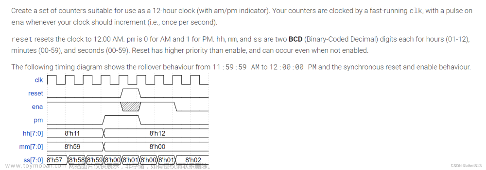
8. 12-hour clock
第三节: Shift Registers
1.
2.
3.
4.
5.
6.
7.
8.
9.
第四节: More Circuits
1.
2.
3.
第五节: Finite State Machines
1.
2.
3.
4.
5.
6.
7.
8.
9.
10.
11.
12.
13.
14.
15.
16.
17.
18.
第三部分: Building Larger Circuits
四、验证阅读模拟 Verification: Reading Simulations
第一部分: Finding bugs in code
第二部分: Build a circuit from a simulation waveform
五、验证编写测试平台 Verification: Writting Testbenches
第一部分: Clock
第二部分: Testbench1
第三部分: AND gate
第四部分: Testbench2
第五部分: T flip-flop
总结
以上就是各单元解法答案。后续会继续更新。文章来源地址https://www.toymoban.com/news/detail-595323.html
到了这里,关于verilog学习 | HDLBits:在线学习答案的文章就介绍完了。如果您还想了解更多内容,请在右上角搜索TOY模板网以前的文章或继续浏览下面的相关文章,希望大家以后多多支持TOY模板网!