Allegro PCB如何显示管脚编号

这篇具有很好参考价值的文章主要介绍了Allegro PCB如何显示管脚编号。希望对大家有所帮助。如果存在错误或未考虑完全的地方,请大家不吝赐教,您也可以点击"举报违法"按钮提交疑问。

显示器件管脚编号方法

器件未显示管脚编号

allegro如何显示元件编号,Allegro PCB设计,硬件工程,pcb工艺,fpga开发,Powered by 金山文档

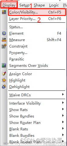
选择Display菜单下的Color/Visibility(颜色/可见性)或按设置的快捷键Alt+Ctrl+C

allegro如何显示元件编号,Allegro PCB设计,硬件工程,pcb工艺,fpga开发,Powered by 金山文档

跳出如下对话框,选择Package Geometry选项→PIN_Number后打钩

allegro如何显示元件编号,Allegro PCB设计,硬件工程,pcb工艺,fpga开发,Powered by 金山文档

设置后器件管脚就显示编号了,效果如下图

allegro如何显示元件编号,Allegro PCB设计,硬件工程,pcb工艺,fpga开发,Powered by 金山文档

博主专注职场硬件设计,如果文章对你有帮助,请关注,点赞,收藏。成长路上有前行者。博主将会定期或不定期分享PADS,Allegro设计技巧和经验。

Allegro provides a good and interactive working interface and powerful functions, and its front-end products Cadence, OrCAD, Capture, the combination of high-speed, high-density, multi-layer complex PCB design routing provides the most perfect solution.

Allegro has perfect Constraint Settings, users only need to set the wiring rules according to the requirements, and the design requirements of the wiring can be achieved without violating the DRC when routing, thus saving the tedious manual inspection time and improving the work efficiency!

It can also define parameters such as minimum wire-width or wire-length to meet the needs of today's high-speed circuit board wiring.

Constraint Manger provides a simple interface for users to set and view Constraint declarations.

Its combination with Capture allows E.E. electronics engineers to set up regular data when drawing a circuit diagram and bring it with them to the Allegro working environment, where it can be automatically processed and checked when placing parts and wiring. The empirical values of these regular data can be reused for the same nature of the circuit board design.

In addition to the above functions, Allegro's powerful automatic push and stick line and perfect automatic repair line function provide users with great convenience;

The powerful mapping function can provide multiple users to deal with a complex board at the same time, thus greatly improving the work efficiency.

Or use the optional graph cutting function to cut the circuit board into various blocks, so that each block has a full-time person at the same time to design, to achieve the purpose of the same graph design and can shorten the time course.

After renaming, online interchange and modifying logic during routing, users can easily return to Capture wiring diagram, and update the wiring diagram to Allegro after modification.

Users can also click and modify objects between Capture and Allegro.文章来源地址https://www.toymoban.com/news/detail-618797.html

到了这里,关于Allegro PCB如何显示管脚编号的文章就介绍完了。如果您还想了解更多内容,请在右上角搜索TOY模板网以前的文章或继续浏览下面的相关文章,希望大家以后多多支持TOY模板网!

本文来自互联网用户投稿,该文观点仅代表作者本人,不代表本站立场。本站仅提供信息存储空间服务,不拥有所有权,不承担相关法律责任。如若转载,请注明出处: 如若内容造成侵权/违法违规/事实不符,请点击违法举报进行投诉反馈,一经查实,立即删除!

领支付宝红包 赞助服务器费用

相关文章

  • 【PCB专题】如何在Allegro中定义字体及批量修改丝印

    在PCB板上丝印往往包含了很多信息,比如元件边界、元件参数、元件编号、极性、静电标识、板号等,这些信息在生产、测试及后期维护等都需要使用。一个好的设计往往都能从丝印的布局、丝印的完整性上体现出来。如下所示PCB在电解电容旁有极性丝印、电阻旁有电阻的位

    2024年02月16日
    浏览(36)
  • Allegro如何在PCB上开槽的三种方法操作指导

    Allegro如何在PCB上开槽的三种方法操作指导 当PCB有特殊设计要求的时候,需要在PCB上开槽,Allegro支持在PCB上开槽操作,具体操作如下 以下图为例,需要在这个板框中间开槽 开方形槽 选择shape add rect命令 画在Board Geometry-outline层,type选择Unfilled 在需要开槽的地方画一个方形的

    2023年04月10日
    浏览(48)
  • Allegro如何在PCB上查看pin number的三种方法操作指导

    Allegro 如何在PCB上查看pin number的三种方法操作指导 Allegro支持快捷的在PCB上查看pin number,如下图 具体操作如下 方法一:show element 选择Show Element命令 Find选择Pins

    2024年02月08日
    浏览(40)
  • allegro pcb 高亮某个网络

    1.调节pcb亮度,点击color192(Ctrl+f5) 点击display ,调低亮度,OK    然后点击 net schedule. 在find栏选择net,在visibility栏all 打钩,然后在pcb选择想要高亮的net,点击一下。 方法二 选择assign net(扫帚) 然后在options栏里选择想高亮的颜色,然后在find栏里选net,然后在visibility栏里

    2024年02月16日
    浏览(29)
  • Allegro如何显示层叠Options和Find操作界面

    Allegro 如何显示层叠Options和Find操作界面   Allegro常规有三大操作界面,层叠,Options和Find,如下图 软件第一次启动的时候,三大界面是关闭的,下面介绍如何把它们打开,具体操作步骤如下 点击菜单上的View 点击Windows

    2024年02月16日
    浏览(28)
  • Allegro-PCB封装更新

    Allegro-封装更新 一、更新所有封装 1、菜单栏-Place-Update Symbol-package symbol-Refresh 二、更新单个封装 1、空白处鼠标右击-Application Mode-placement Edit 选中Placement Edit模式,后选择需要更新封装的器件,右键选择Refresh symbol instance即可 注意,右键在Quick Utilites-Refresh symbol进行更新时和

    2024年02月11日
    浏览(25)
  • Allegro PCB丝印调整,丝印居中

    1,选择File →change editro    2,选择Allegro pcb designer (was performance L ),并勾选Toolbox      ​​​​​​​          3,选择Manufacture →Label tune  4,调整需要放置的位置,居中填入(0.0)坐标即可  5,框选需要调整的丝印,点击Limit layers  我调整的是Assembly层丝印,根据需要选择

    2024年02月11日
    浏览(26)
  • allegro设计PCB操作(记录用)

    目录 NOTES 输入 结构图DXF导入/导出 查看结构图 导入网表 布局 摆放 移动 查看器件坐标 定位器件到指定坐标 与结构图对齐 丝印 布线 测试点/开关等处添加泪滴 高亮 铺铜 电源岛 添加电源岛 编辑电源岛 禁铺区

    2024年02月02日
    浏览(27)
  • Allegro元器件外框丝印突然消失如何解决?Allegro元器件外框丝印显示设置操作步骤

    1.点击Allegro软件左上角Display—Color/Visibility(Ctrl+F5),弹出Color Dialog窗口 2.点击Board Geomentry-----Silkscreen_Bottom和Silkscreen_Top勾选即可,后面颜色框可以修改丝印显示的颜色。 3.点击Apply和OK即可显示元器件外框丝印。 4.元器件外框丝印就会显示成红色。

    2024年02月16日
    浏览(39)
  • Allegro PCB焊盘以及封装制作

    记录硬件工程师的EDA工具学习之路……以Allegro为主…… 表贴焊盘——用于SMD器件,电路板上的“金属铜片” 通孔焊盘——用于直插式器件,包括金属内壁+钻孔 圆焊盘:SC+直径(SC1R00,直径1mm的圆焊盘) 方焊盘:SR+长*宽(SR1R00x1R00,长宽为1mm的方焊盘) 椭圆焊盘:SOB+长*宽

    2024年02月10日
    浏览(27)

觉得文章有用就打赏一下文章作者

支付宝扫一扫打赏

博客赞助

微信扫一扫打赏

请作者喝杯咖啡吧~博客赞助

支付宝扫一扫领取红包,优惠每天领

二维码1

领取红包

二维码2

领红包