前言
INA219 是一款具备 I2C 或 SMBUS 兼容接口的分流器和功率监测计。该器件监测分流器电压降和总线电源电压,转换次数和滤波选项可通过编程设定。可编程校准值与内部乘法器相结合,支持直接读取电流值(单位:安培)。通过附加乘法寄存器可计算功率(单位:瓦)。I2C 或 SMBUS 兼容接口 具有 16 个可编程地址。
INA219 可在 0V 至 26V 范围内感测总线中的分压。该器件由 3V 至 5.5V 单电源供电,电源的最大流耗为1mA。INA219 的工作温度范围为 -40°C 至 125°C。
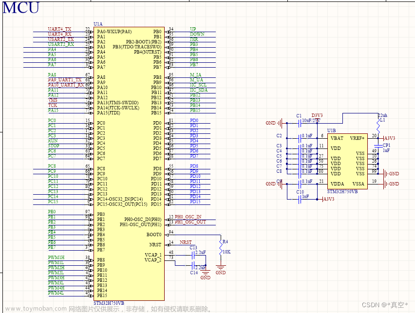
1 原理图

2 IIC地址说明

此测试时A0、A1都下拉接地,所以INA219的IIC通信地址为1000000B
3 寄存器地址说明

- 0x00 配置寄存器,用来配置工作模式、采集范围以及其他参数
- 0x01 分流电阻两端的电压
- 0x02 总线电压(IN-到GND的电压差)
- 0x03 功率
- 0x04 经过分流电阻两端的电流
- 0x05 校准寄存器,用于对测量结果进行校准
4 开始工作前配置
- 0x00 寄存器Bit 13:设置检测最大检测电压 0 = 16V,1 = 32V (此处项目需要测3V到5V的电压,故设置Bit 13 为 0)
- 0x00 寄存器Bit 11-12:设置总线分流电阻最大的电压(此处项目需要测0A到5A的电流,故设置Bit 11-12 为 01,即量程±80mV,可测电流±8A)
- 0x00 寄存器Bit 0-2:设置工作模式(默认)
- 0x05 寄存器:设置基准值(根据需要测的电压、电流范围再套入公式得出结果)
由以下公式可得出0x05的配置值。
C
a
l
=
t
r
u
n
c
(
0.04096
C
u
r
r
e
n
t
L
S
B
×
R
s
h
u
n
t
)
Cal = trunc\left ( \frac{0.04096}{CurrentLSB\times Rshunt} \right )
Cal=trunc(CurrentLSB×Rshunt0.04096)
C
u
r
r
e
n
t
L
S
B
=
M
a
x
i
m
u
m
E
x
p
e
c
t
e
d
C
u
r
r
e
n
t
2
15
CurrentLSB = \frac{Maximum Expected Current}{2^{15}}
CurrentLSB=215MaximumExpectedCurrent文章来源:https://www.toymoban.com/news/detail-767719.html
数据手册说明文档 文章来源地址https://www.toymoban.com/news/detail-767719.html
5 程序代码
1)驱动程序
#include "main.h"
#include "ina219aidcnr_helper.h"

uint16_t ina219_calibrationValue;
uint16_t ina219_currentDivider_mA;
float ina219_powerMultiplier_mW;

/**
 * @brief  The IIC reads 16bit data from the specified register address.
 * @param  ina219 Slave configuration structure of the IIC.
 * @param  registerAddress Internal memory address.
 * @return 16 bit register data.
 */
uint16_t INA219_ReadDataForRegister_16Bits(INA219_t *ina219, uint8_t registerAddress)
{
  uint8_t Value[2];

  HAL_I2C_Mem_Read(ina219->ina219_i2c, (INA219_ADDRESS<<1), registerAddress, 1, Value, 2, 1000);

  return ((Value[0] << 8) | Value[1]);
}

/**
 * @brief  Writes 16 bits of data to the register.
 * @param  ina219 Slave configuration structure of the IIC.
 * @param  registerAddress Internal memory address.
 * @param  Value 16 bits of data to be written.
 */
void INA219_WriteDataToRegister_16Bits(INA219_t *ina219, uint8_t registerAddress, uint16_t Value)
{
  uint8_t regAddr[2];
  /* High Byte */
  regAddr[0] = (Value >> 8) & 0xff;
  /* Low Byte */
  regAddr[1] = (Value >> 0) & 0xff;
  HAL_I2C_Mem_Write(ina219->ina219_i2c, (INA219_ADDRESS<<1), registerAddress, 1, (uint8_t*)regAddr, 2, 1000);
}

/**
 * @brief  Read bus voltage.
 * @param  ina219 Slave configuration structure of the IIC.
 * @return Read voltage value, unit mV.
 */
uint16_t INA219_ReadBusVoltage(INA219_t *ina219)
{
  uint16_t result = INA219_ReadDataForRegister_16Bits(ina219, INA219_REG_BUS_VOLTAGE);

  /* return mV */
  return ((result >> 3  ) * 4);
}

/**
 * @brief  Read current register value.
 * @param  ina219 Slave configuration structure of the IIC.
 * @return Current register value.
 */
uint16_t INA219_ReadCurrentRaw(INA219_t *ina219)
{
  uint16_t result = INA219_ReadDataForRegister_16Bits(ina219, INA219_REG_CURRENT);

  return (result);
}

/**
 * @brief  Read current register value, unit mA.
 * @param  ina219 Slave configuration structure of the IIC.
 * @return Current value.
 */
uint16_t INA219_ReadCurrent_mA(INA219_t *ina219)
{
  uint16_t result = INA219_ReadCurrentRaw(ina219);

  return (result / ina219_currentDivider_mA);
}

/**
 * @brief  Read current register value, unit mV.
 * @param  ina219 Slave configuration structure of the IIC.
 * @return Shunt Voltage value.
 */
uint16_t INA219_ReadShuntVoltage_mV(INA219_t *ina219)
{
  uint16_t result = INA219_ReadDataForRegister_16Bits(ina219, INA219_REG_SHUNT_VOLTAGE);

  /* When multiple sign bits are present, they will all be the same value.
   * Negative numbers are represented in 2's complement format.
   * Generate the 2's complement of a negative number by complementing the absolute value binary number and adding 1.
   * Extend the sign, denoting a negative number by setting the MSB = 1.
   * Extend the sign to any additional sign bits to form the 16-bit word. */
  if(result > MAX_SHUNT_RANGE)
  {
    result = 65536 - MAX_SHUNT_RANGE;
  }

  /* Shunt voltage, unit mV. */
  return (result / 100);
}

/**
 * @brief  INA219 system reset.
 * @param  ina219 Slave configuration structure of the IIC.
 */
void INA219_Reset(INA219_t *ina219)
{
  INA219_WriteDataToRegister_16Bits(ina219, INA219_REG_CONFIG, INA219_CONFIG_RESET);
  HAL_Delay(1);
}

/**
 * @brief Set calibration register.
 * @param ina219 Slave configuration structure of the IIC.
 * @param calibrationData Calibrated data.
 */
void INA219_SetCalibration(INA219_t *ina219, uint16_t calibrationData)
{
  INA219_WriteDataToRegister_16Bits(ina219, INA219_REG_CALIBRATION, calibrationData);
}

/**
 * @brief  Gets the value of the configuration register.
 * @param  ina219 Slave configuration structure of the IIC.
 * @return Configuration Register value.
 */
uint16_t INA219_GetConfigInfo(INA219_t *ina219)
{
  uint16_t result = INA219_ReadDataForRegister_16Bits(ina219, INA219_REG_CONFIG);
  return result;
}

/**
 * @brief Set configuration register.
 * @param ina219 Slave configuration structure of the IIC.
 * @param configData Configuration data.
 */
void INA219_SetConfig(INA219_t *ina219, uint16_t configData)
{
  INA219_WriteDataToRegister_16Bits(ina219, INA219_REG_CONFIG, configData);
}

/**
 * @brief The measurement results are calibrated. Voltage range is 16V, Current range is 8A.
 * @param ina219 Slave configuration structure of the IIC.
 */
void INA219_SetCalibration_16V_8A(INA219_t *ina219)
{
  uint16_t configInfo = INA219_CONFIG_VOLTAGE_RANGE_16V |
                    INA219_CONFIG_GAIN_2_80MV | INA219_CONFIG_BADCRES_12BIT |
                    INA219_CONFIG_SADCRES_12BIT_1S_532US |
                    INA219_CONFIG_MODE_SANDBVOLT_CONTINUOUS;

  // Current_LSB = Maximum Expected Current / 2^15 = (80 / 10) / 2^15 = 0.0002
  // Cal = 0.04096 / (Current_LSB / R) = 0.04096 / (0.0002A * 0.01R) = 20480 = 0x5000
  // Calibration Register = 20480
  ina219_calibrationValue = 20480;

  // 1mA = Current_LSB * bits = 200uA * 5bit (5 bit/mA)
  ina219_currentDivider_mA = 5;
  // 1mW = Power_LSB * bits = 4mW * 0.25bit (0.25f bit/mW)
  ina219_powerMultiplier_mW = 0.25f;

  INA219_SetCalibration(ina219, ina219_calibrationValue);
  INA219_SetConfig(ina219, configInfo);
}

/**
 * @brief  Ina219 driver initialization
 * @param  ina219 Slave configuration structure of the IIC.
 * @param  i2c Pointer to a I2C_HandleTypeDef structure that contains
 *             the configuration information for the specified I2C.
 * @param  Address  Configuration data.
 * @return status.
 */
uint8_t INA219_Init(INA219_t *ina219, I2C_HandleTypeDef *i2c, uint8_t Address)
{
  ina219->ina219_i2c = i2c;
  ina219->Address = Address;

  ina219_currentDivider_mA = 0;
  ina219_powerMultiplier_mW = 0;

  uint8_t ina219_isReady = HAL_I2C_IsDeviceReady(i2c, (Address << 1), 3, 2);

  if(ina219_isReady == HAL_OK)
  {

    INA219_Reset(ina219);
    INA219_SetCalibration_16V_8A(ina219);

    return 1;
  }

  else
  {
    return 0;
  }
}
2)头文件
#ifndef INA219AIDCNR_HELPER_H
#define INA219AIDCNR_HELPER_H


#define INA219_ADDRESS 							        (0x40)
#define MAX_SHUNT_RANGE                     			(0x0FA0)

/* Register */
#define	INA219_REG_CONFIG						        (0x00)
#define	INA219_REG_SHUNT_VOLTAGE				    	(0x01)
#define	INA219_REG_BUS_VOLTAGE					    	(0x02)
#define	INA219_REG_POWER						        (0x03)
#define	INA219_REG_CURRENT						      	(0x04)
#define	INA219_REG_CALIBRATION					    	(0x05)
//
#define INA219_CONFIG_RESET 					      	(0x8000)
//
#define INA219_CONFIG_VOLTAGE_RANGE_16V					(0x0000)      // 0-16V Range
#define INA219_CONFIG_VOLTAGE_RANGE_32V					(0x2000)      // 0-32V Range

#define	INA219_CONFIG_GAIN_1_40MV				    	(0x0000)      // Gain 1, 40mV Range
#define	INA219_CONFIG_GAIN_2_80MV				    	(0x0800)      // Gain 2, 80mV Range
#define	NA219_CONFIG_GAIN_4_160MV				    	(0x1000)      // Gain 4, 160mV Range
#define	INA219_CONFIG_GAIN_8_320MV				  		(0x1800)      // Gain 8, 320mV Range

#define	INA219_CONFIG_BADCRES_9BIT				      	(0x0000)  // 9-bit bus res = 0..511
#define	INA219_CONFIG_BADCRES_10BIT				      	(0x0080)  // 10-bit bus res = 0..1023
#define	INA219_CONFIG_BADCRES_11BIT				      	(0x0100)  // 11-bit bus res = 0..2047
#define	INA219_CONFIG_BADCRES_12BIT				      	(0x0180)  // 12-bit bus res = 0..4097
#define	INA219_CONFIG_BADCRES_12BIT_2S_1060US 			(0x0480)  // 2 x 12-bit bus samples averaged together
#define	INA219_CONFIG_BADCRES_12BIT_4S_2130US	  		(0x0500)  // 4 x 12-bit bus samples averaged together
#define	INA219_CONFIG_BADCRES_12BIT_8S_4260US	  		(0x0580)  // 8 x 12-bit bus samples averaged together
#define	INA219_CONFIG_BADCRES_12BIT_16S_8510US			(0x0600)  // 16 x 12-bit bus samples averaged together
#define	INA219_CONFIG_BADCRES_12BIT_32S_17MS	  		(0x0680)  // 32 x 12-bit bus samples averaged together
#define	INA219_CONFIG_BADCRES_12BIT_64S_34MS	  		(0x0700)  // 64 x 12-bit bus samples averaged together
#define	INA219_CONFIG_BADCRES_12BIT_128S_69MS	  		(0x0780)  // 128 x 12-bit bus samples averaged together

#define	INA219_CONFIG_SADCRES_9BIT_1S_84US		  		(0x0000)  // 1 x 9-bit shunt sample
#define	INA219_CONFIG_SADCRES_10BIT_1S_148US	  		(0x0008)  // 1 x 10-bit shunt sample
#define	INA219_CONFIG_SADCRES_11BIT_1S_276US	  		(0x0010)  // 1 x 11-bit shunt sample
#define	INA219_CONFIG_SADCRES_12BIT_1S_532US	  		(0x0018)  // 1 x 12-bit shunt sample
#define	INA219_CONFIG_SADCRES_12BIT_2S_1060US	  		(0x0048)  // 2 x 12-bit shunt samples averaged together
#define	INA219_CONFIG_SADCRES_12BIT_4S_2130US	  		(0x0050)  // 4 x 12-bit shunt samples averaged together
#define	INA219_CONFIG_SADCRES_12BIT_8S_4260US	 	 	(0x0058)  // 8 x 12-bit shunt samples averaged together
#define	INA219_CONFIG_SADCRES_12BIT_16S_8510US			(0x0060)  // 16 x 12-bit shunt samples averaged together
#define	INA219_CONFIG_SADCRES_12BIT_32S_17MS	  		(0x0068)  // 32 x 12-bit shunt samples averaged together
#define	INA219_CONFIG_SADCRES_12BIT_64S_34MS	  		(0x0070)  // 64 x 12-bit shunt samples averaged together
#define	INA219_CONFIG_SADCRES_12BIT_128S_69MS	  		(0x0078)  // 128 x 12-bit shunt samples averaged together

#define INA219_CONFIG_MODE_MASK					        0x07
#define	INA219_CONFIG_MODE_POWERDOWN			       	0x00
#define	INA219_CONFIG_MODE_SVOLT_TRIGGERED		   		0x01
#define	INA219_CONFIG_MODE_BVOLT_TRIGGERED		   		0x02
#define	INA219_CONFIG_MODE_SANDBVOLT_TRIGGERED	 		0x03
#define	INA219_CONFIG_MODE_ADCOFF				        0x04
#define	INA219_CONFIG_MODE_SVOLT_CONTINUOUS		   		0x05
#define	INA219_CONFIG_MODE_BVOLT_CONTINUOUS		   		0x06
#define	INA219_CONFIG_MODE_SANDBVOLT_CONTINUOUS  		0x07


typedef struct
{
  I2C_HandleTypeDef 	*ina219_i2c;
  uint8_t				Address;
} INA219_t;


uint8_t INA219_Init(INA219_t *ina219, I2C_HandleTypeDef *i2c, uint8_t Address);
uint16_t INA219_ReadBusVoltage(INA219_t *ina219);
uint16_t INA219_ReadCurrent_mA(INA219_t *ina219);
uint16_t INA219_ReadCurrent_raw(INA219_t *ina219);
uint16_t INA219_ReadShuntVoltage_mV(INA219_t *ina219);
uint16_t INA219_ReadDataForRegister_16Bits(INA219_t *ina219, uint8_t registerAddress);
uint16_t INA219_GetConfigInfo(INA219_t *ina219);

void INA219_Reset(INA219_t *ina219);
void INA219_SetCalibration(INA219_t *ina219, uint16_t calibrationData);
void INA219_SetConfig(INA219_t *ina219, uint16_t configData);
void INA219_SetCalibration_16V_8A(INA219_t *ina219);
void INA219_WriteDataToRegister_16Bits(INA219_t *ina219, uint8_t registerAddress, uint16_t Value);


#endif //INA219AIDCNR_HELPER_H
3) 测试代码
int main(void)
{
  /* USER CODE BEGIN 1 */
  uint16_t vbus, vshunt, current;
  /* USER CODE END 1 */

  /* MCU Configuration--------------------------------------------------------*/

  /* Reset of all peripherals, Initializes the Flash interface and the Systick. */
  HAL_Init();

  /* USER CODE BEGIN Init */

  /* USER CODE END Init */

  /* Configure the system clock */
  SystemClock_Config();

  /* USER CODE BEGIN SysInit */

  /* USER CODE END SysInit */

  /* Initialize all configured peripherals */
  MX_GPIO_Init();
  MX_USART1_UART_Init();
  MX_I2C2_Init();
  /* USER CODE BEGIN 2 */

  while(!INA219_Init(&ina219, &hi2c2, INA219_ADDRESS))
  {

  }
  /* USER CODE END 2 */

  /* Infinite loop */
  /* USER CODE BEGIN WHILE */
  while (1)
  {
    /* USER CODE END WHILE */

    /* USER CODE BEGIN 3 */
    vbus = INA219_ReadBusVoltage(&ina219);
    vshunt = INA219_ReadShuntVoltage_mV(&ina219);
    current = INA219_ReadCurrent_mA(&ina219);

    sprintf(strBuffer, "INA219 param: vbus:%d mV; current:%d mA\r\n", vbus, current);
    HAL_UART_Transmit(&huart1, strBuffer, strlen(strDataBuf), 0xff);

    UserDelay_ms(500);
  }
到了这里,关于【STM32 开发】| INA219采集电压、电流值的文章就介绍完了。如果您还想了解更多内容,请在右上角搜索TOY模板网以前的文章或继续浏览下面的相关文章,希望大家以后多多支持TOY模板网!