一、芯片基本信息
SHT30 是瑞士盛世瑞恩生产出品的一个温湿度传感器,该SHT3X是一个系列,一共有SHT30/SHT31/SHT35这三个品类, SHT30——低成本版本,±3% RH精度;SHT31——标准版本,±2% RH精度;RH精度SHT35——高端版本,±1.5% RH;
一般生活内监测用SHT30即可。
SHT30性能参数如下:
温度检测范围:5-60℃
湿度:20%-80%RH
宽电压:2.4-5.5v供电
多种测量模式,具备单次检测/循环检测功能,类似单片机的AD采样
具备温湿度检测自动应答功能(4Hz),这个对于单片机休眠唤醒很有帮助。可以省去RTC唤醒。
具备自检测功能,通过开启加热功能,主动改变设备温度,去确认温湿度传感器是否正常,这个对于无人值守非常有意义。
超低功耗:测量时800uA,待机2uA,更强大的是设备自己具备低功耗管理,无需单片机接入,电池供电必备。
精度越高,对于PCB的走线和设备安装位置要求越高,虽然只有8pin,但是布线不好,安装位置不对,也许还不如热敏电阻的精度。
首先对芯片中对于程序编程有意义的重要信息进行提取:
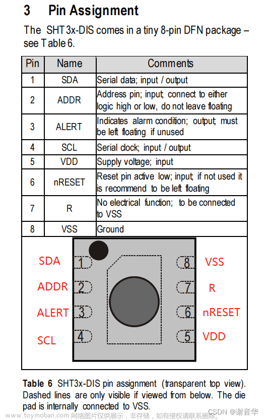
引脚
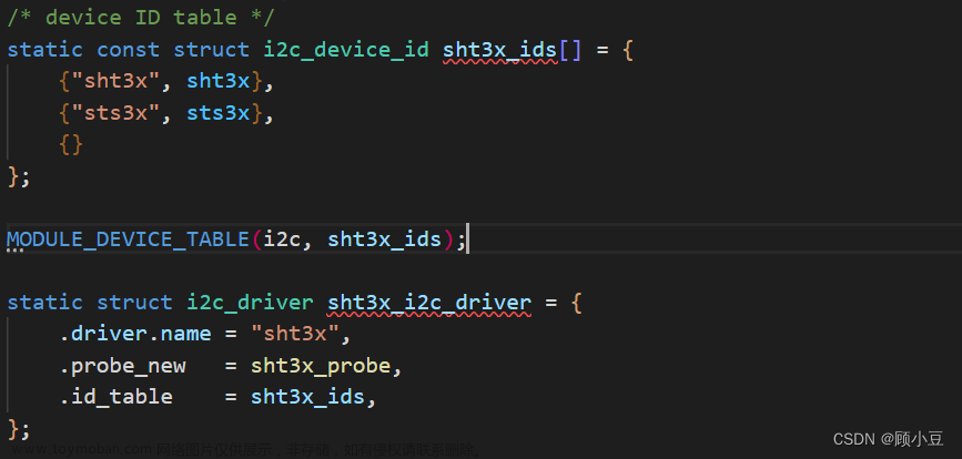
IIC总线挂载芯片区分

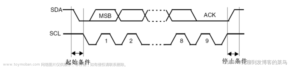
不同模式下的时序配置
根据实际需求选择合适的模式,来进行程序的设计和对应的寄存器配置。

1、Measurement Commands for Single Shot Data Acquisition Mode

2、Readout of Measurement Results for Single Shot Mode

3、Readout of Measurement Results for Periodic Mode

其他
1、软复位命令

2、检验和

3、温度数据计算

二、驱动设计
1- 设计时序
要注意驱动程序中的一些时序信息参数要求,芯片的设计满足的范围,FPGA驱动程序控制时主要注意建立保持时间满足该款芯片的设计指标。具体可以在程序仿真和ILA/逻辑分析仪测试时确定自身驱动程序是否需要优化。


2- 程序控制流程
由于涉及到CRC校验和的情况,对于SHT31温度传感器的设定需要进行控制
根据该时序图的配置模式为设计参考:

IIC的程序调用状态机为以下几个部分(IIC的驱动程序这里不做赘述,百度可复制粘贴 >.^ ):
start → send_byte(0x88) / {7’h44,7’h00}→ wait_ack → send_byte(0x2c) → wait_ack → send_byte(0x06) → wait_ack → stop → delay_us(200) → start → send_byte(0x89) / {7’h44,7’h01} → wait_ack → read_byte(tem[15:8]) → wait_ack → read_byte(temp[7:0]) → send_ack → read_byte(crc) → send_ack → read_byte(hum[15:8]) → send_ack → read_byte(hum[7:0]) → send_ack → read_byte(crc) → send_nack → stop
对于后面的数据不用的,比如只要温度数据,可以直接主机发送NACK结束数据的采集。、
IIC驱动的状态机的顺序如下:

3- 单芯片温湿度数据测试
为了验证程度代码以及芯片的控制方式是否合理,先采用单芯片模式对一个芯片进行控制。
对于中途的仿真和连接芯片后的示波器信号读取后,对细节问题进行优化修改后,测试结果:
① 仿真测试情况
为了验证状态机的设计合理性和调用驱动时是否有错误,需要利用tb仿真文件对代码进行验证。

② ILA数据读取测试情况

③ 示波器测试情况

④ 温湿度数据计算验证
在没有写浮点数值近似处理计算模块前,验证ILA获取的温湿度数据数值是否正常,采用计算机计算即可,ILA上对温湿度数据的显示数值修改为手册中计算的十进制格式。

对第②步中的温湿度数值代入计算后:

所以测试的温湿度计算结果为: 21.9℃ , 40.3% RH。符合实际情况。
4- 双芯片温湿度测试
通过硬件电源接入还是GND接入可使得一组IIC总线上最多能挂载两个芯片,通过以上对单芯片的温湿度数据读取测试中,完善细节后,修改为双芯片控制的配置。

① 仿真测试情况
注意在仿真中需要分别模拟从机芯片SHT31给ACK信号,和不给ACK信号的结果。
给ACK信号时,两个芯片的数据读取整个过程共计消耗2ms的时间(仿真中的数据模拟真实情况下,不同于上述单芯片仿真时为了尽快产生仿真结果模拟缩小后的时间,这里我称 “仿真相对论效应 ” )。

从机给NACK信号时,在芯片1为NACK的时候,对芯片2进行访问控制:

② ILA 测试情况
连接上硬件模块后,ILA抓取实际的信号数据值。

三、可能的风险问题及分析
如果ILA测试中发现一个芯片有ACK然后有数据,一个芯片没ACK或者数据结果全为高(65535)时,需要排查硬件芯片上是否虚焊或者其他可能性,包括代码BUG(如SDA的结束拉高是否进入休眠状态等,在进入休眠状态后又启动的问题)。文章来源:https://www.toymoban.com/news/detail-834654.html
 文章来源地址https://www.toymoban.com/news/detail-834654.html
四、参考代码(只是参考,限于能力毕竟瞎写的)
1- 顶层程序
`timescale 1ns / 1ps
//
// Company:
// Engineer:
//
// Create Date: 2023/01/11 13:45:18
// Design Name: taotao
// Module Name: TOP
// Project Name:
// Target Devices:
// Tool Versions:
// Description:
//
// Dependencies:
//
// Revision:
// Revision 0.01 - File Created
// Additional Comments:
//
//


module TOP(
        input             clk_p,clk_n   ,           // 200M
        input             rst           ,

        output             SCL_A     ,
        inout              SDA_A
    );


    wire            clk_50m ;
    wire            clk_10m ;
    wire            locked  ;
    wire        key_ready_vio;

    wire        [15:0]       rd_data1  ;
    wire        [15:0]       rd_data2  ;

  clk_wiz_0 clk_wiz_0_inst
   (
    // Clock out ports
    .clk_out1_50m(clk_50m),     // output clk_out1_50m
    .clk_out2_10m(clk_10m),     // output clk_out2_10m
    // Status and control signals
    .reset(rst), // input reset
    .locked(locked),       // output locked
   // Clock in ports
    .clk_in1_p(clk_p),    // input clk_in1_p
    .clk_in1_n(clk_n));    // input clk_in1_n

    IOBUF #(
	.DRIVE(12), // Specify the output drive strength
	.IBUF_LOW_PWR("TRUE"),  // Low Power - "TRUE", High Performance = "FALSE"
	.IOSTANDARD("DEFAULT"), // Specify the I/O standard
	.SLEW("SLOW") // Specify the output slew rate
) IOBUF_iic_sdio_A (
	.O     (sda_i_A),     // Buffer output
	.IO    (SDA_A),   // Buffer inout port (connect directly to top-level port)
	.I     (sda_o_A),     // Buffer input
	.T     (~sda_cs_A)      // 3-state enable input, high=input, low=output
);

vio_0   vio_0_inst (
  .clk(clk_50m),                // input wire clk
  .probe_out0(key_ready_vio)  // output wire [0 : 0] probe_out0
);

SHT31_IIC_driver(
       .  clk                       (   clk_50m            )       ,           // 50M for SCL 6.66K
       .  rst                       (   rst            )       ,
       .  I2C_SCL                   (   SCL_A            )       ,
       .  I2C_SDA_out               (   sda_o_A            )       ,
       .  I2C_SDA_in                (   sda_i_A            )       ,
       .  I2C_SDA_oe                (   sda_cs_A            )       ,
       .   ready                    (   key_ready_vio            )       ,            // write and read ready
//       .   tem                      (   rd_data1                )       ,
//       .   hum                      (   rd_data2               )       ,

       .  dout_ack                  (               )       ,         // write data acknowledge by slave device
       .  din_valid                 (               )
);


endmodule
2- 驱动程序
`timescale 1ns / 1ps
//
// Company:
// Engineer:
//
// Create Date: 2023/01/10 18:50:40
// Design Name: taotao
// Module Name: I2C_transmitter
// Project Name:
// Target Devices:
// Tool Versions:
// Description:
//
// Dependencies:
//
// Revision:
// Revision 0.01 - File Created
// Additional Comments:
//
//
module SHT31_IIC_driver(
input clk , // 50M-SCL to give scl 66.66K
input rst ,
output reg I2C_SCL ,
output reg I2C_SDA_out ,
input I2C_SDA_in ,
output reg I2C_SDA_oe ,
input ready , // write and read ready
output reg [15:0] tem1 ,
output reg [15:0] tem2 ,
output reg dout_ack , // write data acknowledge by slave device
// output reg [7:0] din , // for detailed data, it can be changed and given name as belows reg regcognization
output reg din_valid
// input [6:0] dev_addr , // device address
// input [7:0] reg_addr , // register address
// input rdh_wrl , // 1 is read, 0 is write
// input [7:0] dout , // write data
// input [3:0] dout_length , // the number of bytes of write and read data
);
reg [7:0] din ;
reg [7:0] tem_h1 ;
reg [7:0] tem_h2 ;
reg [7:0] tem_l1 ;
reg [7:0] tem_l2 ;
reg [7:0] hum_h ;
reg [7:0] hum_l ;
reg [7:0] crc_tem ;
reg [7:0] crc_hum ;
// reg [15:0] tem ;
reg [15:0] hum ;
// SCL clock generator, 100MHz => 200kHz
reg [11:0] I2C_SCL_counter;
reg I2C_SCL_en; // enable signal, SCL only driven when this one asserted
reg I2C_SCL_d;
wire I2C_SCL_posedge;
wire I2C_SCL_negedge;
//reg [3:0] dout_length = 4'd1;
reg [6:0] dev_addr1 = 7'h44 ;
reg [6:0] dev_addr2 = 7'h45 ;
reg addr_transfer = 1'b0 ;
reg delay_en = 1'b0;
//ila_8 sht_31_inst (
// .clk(clk), // input wire clk
// .probe0( I2C_SCL ), // input wire [0:0] probe0
// .probe1( I2C_SDA_out), // input wire [0:0] probe1
// .probe2( I2C_SDA_in ), // input wire [0:0] probe2
// .probe3( I2C_SDA_oe ), // input wire [0:0] probe3
// .probe4( ready ), // input wire [0:0] probe4
// .probe5( dout_ack ), // input wire [0:0] probe5
// .probe6(din_valid), // input wire [0:0] probe6
// .probe7 (rst ), // input wire [0:0] probe7
// .probe8 (din ), // input wire [7:0] probe8
// .probe9 (tem_h1 ), // input wire [7:0] probe9
// .probe10(tem_l1 ), // input wire [7:0] probe10
// .probe11(tem_h2 ), // input wire [7:0] probe11
// .probe12(tem_l2 ), // input wire [7:0] probe12
// .probe13({addr_transfer,delay_en,crc_hum[7:2]}), // input wire [7:0] probe13
// .probe14(crc_hum), // input wire [7:0] probe14
// .probe15(tem1 ), // input wire [15:0] probe15
// .probe16(tem2 ) // input wire [15:0] probe16
//);
//reg [7:0] reg_addr ;
//reg rdh_wrl ;
always @(posedge clk) begin
if(rst | ~(I2C_SCL_en)) begin
I2C_SCL_counter <= 12'd0;
I2C_SCL <= 1'b1;
end
else if(I2C_SCL_counter < 12'd300) begin // 50M-SCL 100k
// else if(I2C_SCL_counter < 12'd1500) begin // 50M-SCL 20k
// else if(I2C_SCL_counter < 12'd150) begin // 50M-SCL 200K
I2C_SCL_counter <= I2C_SCL_counter + 12'd1;
end
else begin
I2C_SCL_counter <= 12'd0;
I2C_SCL <= ~I2C_SCL;
end
end
// detection of falling edge of SCL
always @(posedge clk) begin
I2C_SCL_d <= I2C_SCL;
end
assign I2C_SCL_negedge = ({I2C_SCL_d,I2C_SCL}==2'b10) ? 1'b1 : 1'b0;
assign I2C_SCL_posedge = ({I2C_SCL_d,I2C_SCL}==2'b01) ? 1'b1 : 1'b0;
// ready rising edge detection
reg ready_d;
wire ready_posedge;
always @(posedge clk) begin
ready_d <= ready;
end
assign ready_posedge = ({ready_d, ready}==2'b01) ? 1'b1 : 1'b0;
// state machine
//parameter [3:0] IDLE = 0;
//parameter [3:0] START = 1;
//parameter [3:0] ADDR_DEV_WRITE = 2;
//parameter [3:0] ADDR_REG = 3;
//parameter [3:0] REPEAT_START = 4;
//parameter [3:0] ADDR_DEV_READ = 5;
//parameter [3:0] WRITE = 6;
//parameter [3:0] READ = 7;
//parameter [3:0] ENDING = 8;
localparam IDLE = 5'd00 ,
START_1 = 5'd01 ,
SEND_ADDR_W = 5'd02 , //0x88
ACK_1 = 5'd03 ,
SEND_COM_H = 5'd04 , //0x2c
ACK_2 = 5'd05 ,
SEND_COM_L = 5'd06 , //0x06
ACK_3 = 5'd07 ,
STOP = 5'd08 ,
DELAY_1 = 5'd09 , //500ms
START_2 = 5'd10 ,
SEND_ADDR_R = 5'd11 , //0x89
ACK_4 = 5'd12 ,
READ_TEM_H = 5'd13 ,
ACK_5 = 5'd14 ,
READ_TEM_L = 5'd15 ,
ACK_6 = 5'd16 ,
READ_CRC_1 = 5'd17 ,
ACK_7 = 5'd18 ,
READ_HUM_H = 5'd19 ,
ACK_8 = 5'd20 ,
READ_HUM_L = 5'd21 ,
ACK_9 = 5'd22 ,
READ_CRC_2 = 5'd23 ,
NACK = 5'd24 ,
END_STOP = 5'd25 ,
ENDING = 5'd26 ,
DELAY = 5'd27 ;
reg [4:0] state;
reg [4:0] next_state;
reg [3:0] I2C_SCL_count;
reg [7:0] dout_buf;
reg [3:0] dout_count;
reg [7:0] din_buf;
reg [7:0] din_buf1;
reg [7:0] din_buf2;
reg [12:0] end_count;
reg [27:0] delay_cnt = 28'd0 ;
always @(posedge clk or posedge rst) begin
if(rst) begin
state <= IDLE;
end
else begin
state <= next_state;
end
end
always @(posedge clk) begin
case(state)
IDLE: begin
dout_ack <= 1'b0;
I2C_SCL_count <= 4'd0;
din <= 8'h00;
din_valid <= 1'b0;
I2C_SDA_out <= 1'b1;
I2C_SDA_oe <= 1'b0;
// next_state <= START_1;
dout_buf <= 8'h00;
I2C_SCL_en <= 1'b0;
dout_count <= 4'd0;
end_count <= 13'd0;
if(addr_transfer) begin
if(delay_cnt >= 28'd25000) begin // 500us
// if(delay_cnt >= 28'd2500) begin // 50us for simulation
delay_cnt <= 28'd0;
next_state <= START_1;
end else begin
delay_cnt <= delay_cnt + 1'b1;
// next_state <= IDLE; // �����ڴ˴����Ӹ���䣬������ظ�ִ�и�״̬
end
end else begin
next_state <= START_1;
end
end
START_1: begin
if(ready_posedge || addr_transfer) begin
next_state <= SEND_ADDR_W;
I2C_SDA_out <= 1'b0;
I2C_SDA_oe <= 1'b0;
I2C_SCL_en <= 1'b1;
if(!addr_transfer) begin
dout_buf <= {dev_addr1, 1'b0}; // the first step is always write register address
end else if(addr_transfer) begin
dout_buf <= {dev_addr2, 1'b0};
end
// dout_buf <= {dev_addr2, 1'b0}; // IIC does not support get both data at the same time
end
end
SEND_ADDR_W: begin
if(I2C_SCL_negedge && (I2C_SCL_count < 4'd8) ) begin
I2C_SCL_count <= I2C_SCL_count + 4'd1;
{I2C_SDA_out, dout_buf} <= {dout_buf, 1'b0};
I2C_SDA_oe <= 1'b0;
end
else if(I2C_SCL_negedge && (I2C_SCL_count == 4'd8)) begin
I2C_SCL_count <= I2C_SCL_count + 4'd1;
I2C_SDA_oe <= 1'b1;
// I2C_SDA_out<= 1'b1;
end
else if(I2C_SCL_posedge && (I2C_SCL_count == 4'd9)) begin
I2C_SCL_count <= 4'd0;
// dout_buf <= 8'h24;
dout_buf <= 8'h2c;
if(~I2C_SDA_in) begin // acknowledged by device and turn to ADDR_REG state
next_state <= SEND_COM_H;
end
else begin // not acknowledged, go to ENDING
next_state <= ENDING;
if(addr_transfer) begin
addr_transfer <= 1'b0;
end else if(!addr_transfer) begin
addr_transfer <= 1'b1;
end
end
end
end
SEND_COM_H: begin
if(I2C_SCL_negedge && (I2C_SCL_count < 4'd8) ) begin
I2C_SCL_count <= I2C_SCL_count + 4'd1;
{I2C_SDA_out, dout_buf} <= {dout_buf, 1'b0};
I2C_SDA_oe <= 1'b0;
end
else if(I2C_SCL_negedge && (I2C_SCL_count == 4'd8)) begin
I2C_SCL_count <= I2C_SCL_count + 4'd1;
I2C_SDA_oe <= 1'b1;
// I2C_SDA_out<= 1'b1;
end
else if(I2C_SCL_posedge && (I2C_SCL_count == 4'd9)) begin
I2C_SCL_count <= 4'd0;
// dout_buf <= 8'h0B;
dout_buf <= 8'h06;
if(~I2C_SDA_in) begin // acknowledged by device and turn to ADDR_REG state
next_state <= SEND_COM_L;
end
else begin // not acknowledged, go to ENDING
next_state <= ENDING;
end
end
end
SEND_COM_L: begin
if(I2C_SCL_negedge && (I2C_SCL_count < 4'd8) ) begin
I2C_SCL_count <= I2C_SCL_count + 4'd1;
{I2C_SDA_out, dout_buf} <= {dout_buf, 1'b0};
I2C_SDA_oe <= 1'b0;
end
else if(I2C_SCL_negedge && (I2C_SCL_count == 4'd8)) begin
I2C_SCL_count <= I2C_SCL_count + 4'd1;
I2C_SDA_oe <= 1'b1;
end
else if(I2C_SCL_posedge && (I2C_SCL_count == 4'd9)) begin
I2C_SCL_count <= 4'd0;
if( ~I2C_SDA_in) begin // acknowledged by device and turn to read state
next_state <= STOP;
// I2C_SDA_oe <= 1'b0;
// I2C_SDA_out <= 1'b1;
if(!addr_transfer) begin
dout_buf <= {dev_addr1, 1'b1}; // the first step is always write register address
end else if(addr_transfer) begin
dout_buf <= {dev_addr2, 1'b1};
end
end
// else if(~rdh_wrl && ~I2C_SDA_in) begin // acknowledged by device and turn to write state
// next_state <= WRITE;
// dout_buf <= dout;
// end
else begin // not acknowledged, go to ENDING
next_state <= ENDING;
end
// I2C_SDA_oe <= 1'b0;
end
end
STOP: begin
// not stopped by master
if(I2C_SCL_negedge) begin
I2C_SDA_oe <= 1'b0;
I2C_SDA_out <= 1'b0;
end
else if(I2C_SCL_posedge) begin // delay 10us to make sda high
I2C_SCL_en <= 1'b0;
delay_en <= 1'b1;
// I2C_SDA_out <= 1'b1;
// delay a while and pull down the SDA, indicating repeat start
end else if(delay_cnt >= 28'd400) begin
delay_cnt <= 1'd0;
I2C_SDA_out <= 1'b1;
delay_en <= 1'b0;
end else if(delay_en) begin
delay_cnt <= delay_cnt + 1'b1;
end else if(~I2C_SCL_en && (end_count < 13'd5000)) begin //100us
end_count <= end_count + 13'd1;
end else if(~I2C_SCL_en) begin
end_count <= 13'd0;
I2C_SCL_en <= 1'b1;
I2C_SDA_out <= 1'b0;
next_state <= SEND_ADDR_R;
end else begin
// delay_cnt <= delay_cnt + 1'b1;
end
end
// SEND_COM_L: begin
// if(I2C_SCL_negedge && (I2C_SCL_count < 4'd8) ) begin
// I2C_SCL_count <= I2C_SCL_count + 4'd1;
// {I2C_SDA_out, dout_buf} <= {dout_buf, 1'b0};
// I2C_SDA_oe <= 1'b0;
// end
// else if(I2C_SCL_negedge && (I2C_SCL_count == 4'd8)) begin
// I2C_SCL_count <= I2C_SCL_count + 4'd1;
// I2C_SDA_oe <= 1'b1;
I2C_SDA_out<= 1'b1;
// end
// else if(I2C_SCL_posedge && (I2C_SCL_count == 4'd9)) begin
// I2C_SCL_count <= 4'd0;
// if(~I2C_SDA_in) begin // acknowledged by device and turn to ADDR_REG state
// next_state <= STOP;
I2C_SDA_out <= 1'b1;
// I2C_SDA_oe <= 1'b0;
// end
// else begin // not acknowledged, go to ENDING
// next_state <= ENDING;
// end
// end
// end
// STOP: begin
// dout_ack <= 1'b0;
// I2C_SCL_count <= 4'd0;
// din <= 8'h00;
// din_valid <= 1'b0;
// I2C_SDA_out <= 1'b1;
// I2C_SDA_oe <= 1'b0;
// next_state <= DELAY_1;
// dout_buf <= 8'h00;
// I2C_SCL_en <= 1'b0;
// dout_count <= 4'd0;
// end_count <= 8'd0;
// end
// DELAY_1:begin
if(delay_cnt >= 28'd25_000_000) begin // 500ms
if(delay_cnt >= 28'd25000) begin // 500us for tb simulation
// if(delay_cnt >= 28'd2500) begin // 50us for tb simulation
// delay_cnt <= 28'd0;
// next_state <= START_2;
// end else begin
// delay_cnt <= delay_cnt + 1'd1;
// end
// end
// START_2: begin
// next_state <= SEND_ADDR_R;
// dout_buf <= {dev_addr, 1'b1}; // the first step is always write register address
// I2C_SDA_out <= 1'b0;
// I2C_SDA_oe <= 1'b0;
// I2C_SCL_en <= 1'b1;
// end
SEND_ADDR_R: begin
if(I2C_SCL_negedge && (I2C_SCL_count < 4'd8) ) begin
I2C_SCL_count <= I2C_SCL_count + 4'd1;
{I2C_SDA_out, dout_buf} <= {dout_buf, 1'b0};
I2C_SDA_oe <= 1'b0;
end
else if(I2C_SCL_negedge && (I2C_SCL_count == 4'd8)) begin
I2C_SCL_count <= I2C_SCL_count + 4'd1;
I2C_SDA_oe <= 1'b1; // master send ack to slaver
end
else if(I2C_SCL_posedge && (I2C_SCL_count == 4'd9)) begin
I2C_SCL_count <= 4'd0;
if(~I2C_SDA_in) begin // acknowledged by device and turn to ADDR_REG state
next_state <= READ_TEM_H;
// I2C_SDA_oe <= 1'b1;
end
else begin // not acknowledged, go to ENDING
next_state <= STOP;
end
end
end
READ_TEM_H: begin
if(I2C_SCL_posedge && (I2C_SCL_count < 4'd8) ) begin
I2C_SCL_count <= I2C_SCL_count + 4'd1;
// din_buf <= {din_buf[6:0], I2C_SDA_in};
din_valid <= 1'b0;
I2C_SDA_oe <= 1'b1;
if(!addr_transfer) begin
din_buf1 <= {din_buf1[6:0], I2C_SDA_in};
end else if(addr_transfer) begin
din_buf2 <= {din_buf2[6:0], I2C_SDA_in};
end
end
else if(I2C_SCL_negedge && (I2C_SCL_count == 4'd8)) begin
I2C_SCL_count <= I2C_SCL_count + 4'd1;
din_valid <= 1'b1;
I2C_SDA_oe <= 1'b0;
I2C_SDA_out <= 1'b0; // send ack to salver
if(!addr_transfer) begin
din <= din_buf1; // because not assure this data, should give it detailed name like tem_h
tem_h1 <= din_buf1;
end else if(addr_transfer) begin
din <= din_buf2; // because not assure this data, should give it detailed name like tem_h
tem_h2 <= din_buf2;
end
end
else if(I2C_SCL_negedge && (I2C_SCL_count == 4'd9)) begin
I2C_SCL_count <= 4'd0;
I2C_SDA_oe <= 1'b1;
// if(dout_count == (dout_length - 4'd1) ) begin // already read enough, go to next
next_state <= READ_TEM_L;
dout_count <= 4'd0;
// end
// else begin // need more data, continue in READ state
// next_state <= READ_TEM_H;
// dout_count <= dout_count + 4'd1;
// end
end
else begin
din_valid <= 1'b0;
end
end
READ_TEM_L:begin
if(I2C_SCL_posedge && (I2C_SCL_count < 4'd8) ) begin
I2C_SCL_count <= I2C_SCL_count + 4'd1;
din_valid <= 1'b0;
I2C_SDA_oe <= 1'b1;
if(!addr_transfer) begin
din_buf1 <= {din_buf1[6:0], I2C_SDA_in};
end else if(addr_transfer) begin
din_buf2 <= {din_buf2[6:0], I2C_SDA_in};
end
end
else if(I2C_SCL_negedge && (I2C_SCL_count == 4'd8)) begin
I2C_SCL_count <= I2C_SCL_count + 4'd1;
din_valid <= 1'b1;
I2C_SDA_oe <= 1'b0;
I2C_SDA_out <= 1'b1; // send nack to salver ,and end to get temp
if(!addr_transfer) begin
din <= din_buf1; // because not assure this data, should give it detailed name like tem_h
tem_l1 <= din_buf1;
end else if(addr_transfer) begin
din <= din_buf2; // because not assure this data, should give it detailed name like tem_h
tem_l2 <= din_buf2;
end
end
else if(I2C_SCL_negedge && (I2C_SCL_count == 4'd9)) begin
I2C_SCL_count <= 4'd0;
// I2C_SDA_oe <= 1'b1;
// next_state <= READ_CRC_1; // enough for temp
I2C_SDA_oe <= 1'b0;
I2C_SDA_out <= 1'b0;
next_state <= END_STOP;
dout_count <= 4'd0;
if(!addr_transfer) begin
tem1 <= {tem_h1,tem_l1}; // to build this temperature after get the data of tem_h and tem_l
addr_transfer <= 1'b1;
end else if(addr_transfer) begin
tem2 <= {tem_h2,tem_l2};
addr_transfer <= 1'b0;
end
end
else begin
din_valid <= 1'b0;
end
end
READ_CRC_1:begin
if(I2C_SCL_posedge && (I2C_SCL_count < 4'd8) ) begin
I2C_SCL_count <= I2C_SCL_count + 4'd1;
din_buf <= {din_buf[6:0], I2C_SDA_in};
din_valid <= 1'b0;
I2C_SDA_oe <= 1'b1;
end
else if(I2C_SCL_negedge && (I2C_SCL_count == 4'd8)) begin
I2C_SCL_count <= I2C_SCL_count + 4'd1;
// din <= din_buf;
crc_tem <= din_buf;
din_valid <= 1'b1;
I2C_SDA_oe <= 1'b0;
I2C_SDA_out <= 1'b0; // send ack to salver
end
else if(I2C_SCL_negedge && (I2C_SCL_count == 4'd9)) begin
I2C_SCL_count <= 4'd0;
I2C_SDA_oe <= 1'b1;
next_state <= READ_HUM_H;
dout_count <= 4'd0;
end
else begin
din_valid <= 1'b0;
end
end
READ_HUM_H:begin
if(I2C_SCL_posedge && (I2C_SCL_count < 4'd8) ) begin
I2C_SCL_count <= I2C_SCL_count + 4'd1;
din_buf <= {din_buf[6:0], I2C_SDA_in};
din_valid <= 1'b0;
I2C_SDA_oe <= 1'b1;
end
else if(I2C_SCL_negedge && (I2C_SCL_count == 4'd8)) begin
I2C_SCL_count <= I2C_SCL_count + 4'd1;
// din <= din_buf;
hum_h <= din_buf;
din_valid <= 1'b1;
I2C_SDA_oe <= 1'b0;
I2C_SDA_out <= 1'b0; // send ack to salver
end
else if(I2C_SCL_negedge && (I2C_SCL_count == 4'd9)) begin
I2C_SCL_count <= 4'd0;
I2C_SDA_oe <= 1'b1;
next_state <= READ_HUM_L;
dout_count <= 4'd0;
end
else begin
din_valid <= 1'b0;
end
end
READ_HUM_L:begin
if(I2C_SCL_posedge && (I2C_SCL_count < 4'd8) ) begin
I2C_SCL_count <= I2C_SCL_count + 4'd1;
din_buf <= {din_buf[6:0], I2C_SDA_in};
din_valid <= 1'b0;
I2C_SDA_oe <= 1'b1;
end
else if(I2C_SCL_negedge && (I2C_SCL_count == 4'd8)) begin
I2C_SCL_count <= I2C_SCL_count + 4'd1;
// din <= din_buf;
hum_l <= din_buf;
din_valid <= 1'b1;
I2C_SDA_oe <= 1'b0;
I2C_SDA_out <= 1'b0; // send ack to salver
end
else if(I2C_SCL_negedge && (I2C_SCL_count == 4'd9)) begin
I2C_SCL_count <= 4'd0;
I2C_SDA_oe <= 1'b1;
next_state <= READ_CRC_2;
dout_count <= 4'd0;
hum <= {hum_h,hum_l}; // to build this temperature after get the data of hum_h and hum_l
end
else begin
din_valid <= 1'b0;
end
end
READ_CRC_2:begin
if(I2C_SCL_posedge && (I2C_SCL_count < 4'd8) ) begin
I2C_SCL_count <= I2C_SCL_count + 4'd1;
din_buf <= {din_buf[6:0], I2C_SDA_in};
din_valid <= 1'b0;
I2C_SDA_oe <= 1'b1;
end
else if(I2C_SCL_negedge && (I2C_SCL_count == 4'd8)) begin
I2C_SCL_count <= I2C_SCL_count + 4'd1;
// din <= din_buf;
crc_hum <= din_buf;
din_valid <= 1'b1;
I2C_SDA_oe <= 1'b0;
I2C_SDA_out <= 1'b1; // send nack to salver
end
else if(I2C_SCL_negedge && (I2C_SCL_count == 4'd9)) begin
I2C_SCL_count <= 4'd0;
I2C_SDA_oe <= 1'b0;
I2C_SDA_out <= 1'b0;
next_state <= END_STOP;
dout_count <= 4'd0;
end
else begin
din_valid <= 1'b0;
end
end
END_STOP:begin
if(I2C_SCL_posedge) begin
I2C_SCL_en <= 1'b0;
I2C_SDA_oe <= 1'b0;
delay_en <= 1'b1;
// I2C_SDA_out <= 1'b1;
// delay a while and pull down the SDA, indicating repeat start
end else if(delay_cnt >= 28'd400) begin
delay_cnt <= 1'd0;
I2C_SDA_out <= 1'b1;
delay_en <= 1'b0;
end else if(delay_en) begin
delay_cnt <= delay_cnt + 1'b1;
// delay a while and pull up the SDA, indicating the end
end else if(~I2C_SCL_en && (end_count < 13'd250)) begin
end_count <= end_count + 13'd1;
end
else if(~I2C_SCL_en) begin
I2C_SDA_oe <= 1'b0;
I2C_SDA_out <= 1'b1;
next_state <= IDLE;
end_count <= 13'd0;
end
end
// DELAY : begin
// delay_cnt <= delay_cnt + 1'd1;
if(delay_cnt >= 28'd25000) begin // 500us
// if(delay_cnt >= 28'd100) begin // 50us for simulation
// delay_cnt <= 28'd0;
// next_state <= IDLE;
// end else begin
// next_state <= DELAY;
// end
// end
ENDING: begin
if(I2C_SCL_posedge) begin
I2C_SCL_en <= 1'b0;
I2C_SDA_oe <= 1'b0;
delay_en <= 1'b1;
// I2C_SDA_out <= 1'b1;
// delay a while and pull down the SDA, indicating repeat start
end else if(delay_cnt >= 28'd400) begin
delay_cnt <= 1'd0;
I2C_SDA_out <= 1'b1;
delay_en <= 1'b0;
end else if(delay_en) begin
delay_cnt <= delay_cnt + 1'b1;
// delay a while and pull up the SDA, indicating the end
end else if(~I2C_SCL_en && (end_count < 13'd250)) begin
end_count <= end_count + 13'd1;
end
else if(~I2C_SCL_en) begin
I2C_SDA_out <= 1'b1;
next_state <= IDLE;
end
end
endcase
end
//ila_0_druver your_instance_name (
// .clk(clk), // input wire clk
// .probe0 (I2C_SCL ), // input wire [0:0] probe0
// .probe1 (I2C_SDA_out ), // input wire [0:0] probe1
// .probe2 (I2C_SDA_in ), // input wire [0:0] probe2
// .probe3 (I2C_SDA_oe ), // input wire [0:0] probe3
// .probe4 ( dev_addr ), // input wire [6:0] probe4
// .probe5 ( reg_addr ), // input wire [7:0] probe5
// .probe6 ( rdh_wrl ), // input wire [0:0] probe6
// .probe7 ( ready ), // input wire [0:0] probe7
// .probe8 ( dout ), // input wire [7:0] probe8
// .probe9 ( dout_ack ), // input wire [0:0] probe9
// .probe10 ( dout_length ), // input wire [3:0] probe10
// .probe11 ( din ), // input wire [7:0] probe11
// .probe12 ( din_valid ) // input wire [0:0] probe12
//);
endmodule3- 仿真程序
`timescale 1ns / 1ps
//
// Company:
// Engineer:
//
// Create Date: 2022/12/22 16:42:31
// Design Name: taotao
// Module Name: tb_sht31_i2c
// Project Name:
// Target Devices:
// Tool Versions:
// Description:
//
// Dependencies:
//
// Revision:
// Revision 0.01 - File Created
// Additional Comments:
//
//


module tb_sht31_i2c();

    reg     clk         ;
    reg     rst         ;
    reg     I2C_SDA_in  ;
    reg     ready       ;

    initial begin
        clk             =           1'b0    ;
        rst             =           1'b1    ;
        I2C_SDA_in      =           1'b1    ;
        ready           =           1'b0    ;

        #200
        rst             =           1'b0    ;
        #500
        ready           =           1'b1    ;
        #200
        ready           =           1'b0    ;
        #100
        I2C_SDA_in      =           1'b0    ;         // if ack
//        I2C_SDA_in      =           1'b1    ;       // if nack
    end

        always #10  clk = ~clk;

    SHT31_IIC_driver    SHT31_IIC_driver_inst(
            .clk                        (  clk                      )   ,
            .rst                        (  rst                      )   ,
            .I2C_SCL                    (  I2C_SCL                  )   ,
            .I2C_SDA_out                (  I2C_SDA_out              )   ,
            .I2C_SDA_in                 (  I2C_SDA_in               )   ,
            .I2C_SDA_oe                 (  I2C_SDA_oe               )   ,
            .ready                      (  ready                    )   ,            // write and read ready
            .dout_ack                   (  dout_ack                 )   ,         // write data acknowledge by slave device
//            .din                        (  din                      )   ,
            .din_valid                  (  din_valid                )
        );

endmodule
到了这里,关于FPGA读取SHT31温湿度传感器的文章就介绍完了。如果您还想了解更多内容,请在右上角搜索TOY模板网以前的文章或继续浏览下面的相关文章,希望大家以后多多支持TOY模板网!